SCD Digitization
Overview
The SCDDigi algorithm consists of three main components: the calculation of charge distribution on implemented strips, the consideration of coupling effects caused by capacitive net, and the modeling of electronic response.
Charge distribution
The charge distribution on implant strips is determined using the Belau model, which aggregates multiple Gaussian distributions. The diffusion radius can be adjusted to fine-tune the accuracy of the calculation. The formula of diffusion is
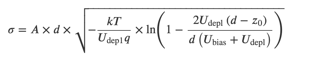
where k is the Boltzmann constant, T is the effective temperature, q is the meta charge, U~depl~ is the silicon detector depletion voltage, U~bias~ is the internal applied bias voltage to the detector, d is the detector thickness, z~0~ is z coordinate when electron-hole pair is created and A is diffusionCoefficient. The default value of A in the code is 1.
Schematic diagram of the calculation of charge distribution is below.
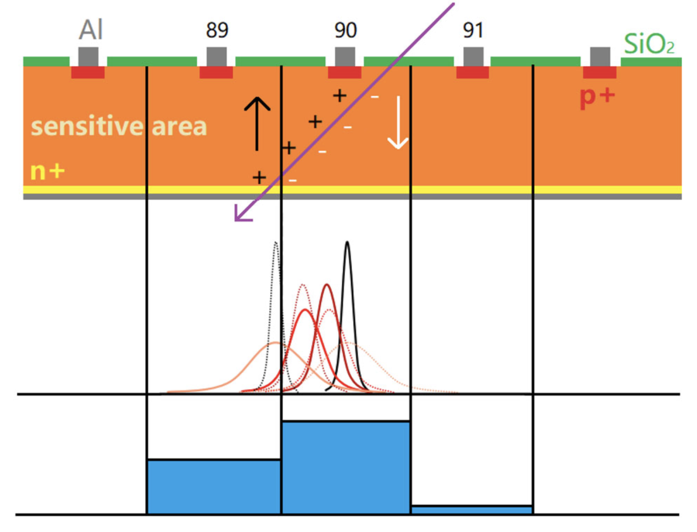
The upper panel indicates the schematic diagram of the silicon strip detector, the middle panel denotes the Gaussian function of each part that represents the space distribution of electrons/holes that accumulated on the surface, the solid curves represent the holes and the dotted curves represent the electrons, the black vertical lines indicate the boundary of each strip and the lower panel represents the space distribution of the electrons/holes accumulated at the implanted strips.
Coupling effects
The calculation of the charge coupling coefficient can be done through two methods by controlling the directCoe: either by considering the capacitance or by directly utilizing coefficients from 2018 beam test data.
The capacitive coupling network is schematically shown belowŁ¬
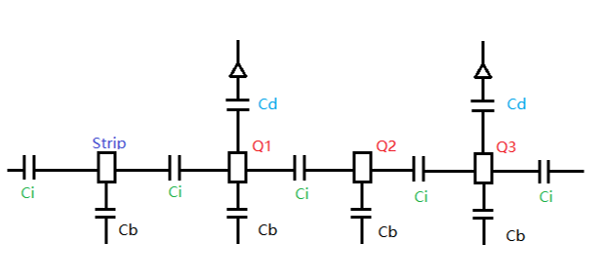
where C~i~ is a capacitance between implant strip, C~b~ is a decoupling capacitance and C~d~ is a capacitance to backplane-guardring. These three capacitances are interCapa ,doupCapa , backCapa in code, respectively.
Coefficients from beam test data are readoutCapaCoupEffi0, readoutCapaCoupEffi1, readoutCapaCoupEffi2, floatCapaCoupEffi0 and floatCapaCoupEffi1. The more detailed descriptions of these variables are provided in the table below.
Electronic response
The charge of sensor in the same ladder (same ladderid which is ladderid = cellcode/100 ) is added together.
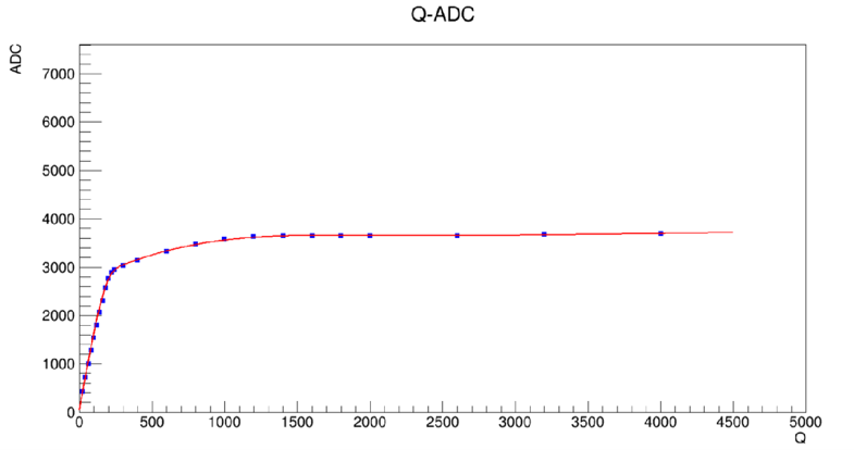
The electronic response is modeled using a spline function, which converts the corresponding deposited charge to the analog-to-digital converter (ADC) value. The function of Q to ADC is provided by hardware measurement. This step ensures an accurate representation of the signal detected by the electronics.
Noise and baseline
The default in the code is to subtract the baseline which is from the spline function. In this case, the ADC which is greater than the baseline value + noiseThreshold*noise will be saved. If we choose not to subtract the baseline, all the ADC will be saved to the output.
Adjustable parameters
As shown in the table below, the explanation of adjustable parameters is provided.
name |
type |
description |
default |
|---|---|---|---|
inputcoll |
string |
inputCollName |
ˇ°scdhitsˇ± |
outputcoll |
string |
outputCollName |
ˇ°scddigiˇ± |
implantPitch |
double |
implant strip pitch |
100(um) |
readoutPitch |
double |
readout strip pitch |
200(um) |
interCapa |
double |
the capacitance between implant strip |
4.4(pF) |
doupCapa |
double |
the decoupling capacitance |
510(pF) |
backCapa |
double |
the capacitance to backplane-guardring |
4.3(pF) |
readoutCapaCoupEffi0 |
double |
the coupling coefficient to the same readout strip that charge deposited |
0.83 |
readoutCapaCoupEffi1 |
double |
the coupling coefficient to the neibouring readout strip when charge deposited at readout strip |
0.07 |
readoutCapaCoupEffi2 |
double |
the coupling coefficient to the two neighboring readout strip when charge deposited at readout strip |
0.015 |
floatCapaCoupEffi0 |
double |
the coupling coefficient to the neibouring readout strip when charge deposited at non-readout strip |
0.18 |
floatCapaCoupEffi1 |
double |
the coupling coefficient to the two neighboring readout strip when charge deposited at non-readout strip |
0.027 |
belauMinDiffusion |
double |
the minimum diffusion radius |
1(um) |
diffusionCoefficient |
double |
an artifitial parameter to change the diffusion coefficient |
1 |
subtractBaseline |
bool |
subtracting the pedestal or not for the output ADC |
True |
primaryOnly |
bool |
whether just output the ADC generated by primary particle, default is false |
False |
noise |
double |
the sigma of gaus of noise distribution |
3(ADC) |
noiseThreshold |
double |
the threshold for baseline substraction |
4(sigma) |
directCoe |
bool |
use mCi,mCd,mCb to calculate the coupling effect of capacitive net when itˇŻs false, use mRCCE_0,mRCCE_1,ˇ to calculate the coupling effect of capacitive net when itˇŻs true |
False |
Output
The output of the digization is a edm::SiliconDigiHit of name defaults to scddigi, which include the cellcode of ladder, stripID and ADC value for each strip.
Usage Example
  import SCDDigi
  scddigi = task.createAlg("SCDDigi_v1")